| _________ |
 |
__________ | |||||||||||||||||||||||||||||||||||||||||||||||||||||||||||||
| FDIB Scientific E-Zine @ 1-2001 | |||||||||||||||||||||||||||||||||||||||||||||||||||||||||||||||
| A
New Preparation Method for Sputtered MoO3 Multilayers for the
Application in Gas Sensors
C. Imawan, H. Steffes, F. Solzbacher, E. Obermeier Technical University
of Berlin, Microsensor & Actuator Technology (MAT),
Abstract A new method for the preparation of sputtered MoO3 multilayer thin films for the application in gas sensors has been developed. A remarkable change of the crystallinity and the microstructure compared to the whisker-like structure of conventionally sputtered MoO3 single-layer films is found. The multilayer films have a dense and a smooth structure with a small crystallite size. This preparation method evidences that the H2 sensing properties such as sensitivity, selectivity, response time and long-term stability of the sensors can be improved. The cross-sensitivity towards NO2, NH3, CO, CH4, and SO2 is low. The response time (t50) to H2 can be drastically reduced from 40 s for the single-layer film to 10 s. The sensor exposes a very high response to H2 with a good signal linearity for high concentrations ranging from 2000 to 9000 ppm. Keywords: Sputtering; MoO3 multilayer; H2 gas sensors 1. Introduction
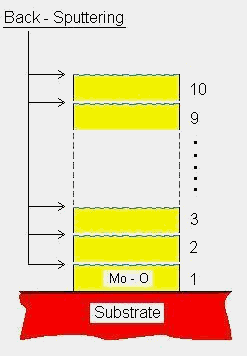
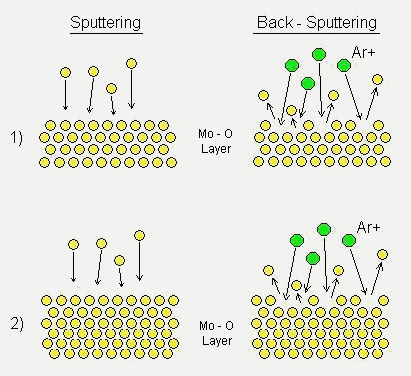
For the preparation of the MoO3 multilayer successive processes of sputtering and back-sputtering are developed. A major advantage of this technique is that a back-sputtering process at each interface during the multilayer deposition leads to interfacial diffusion of atoms but not leading to any substantial increase in crystal structure development. Therefore, the films show a dense structure and a smooth surface with reduced crystallite sizes. It is evident that the structure can improve the long-term stability of the sensors without reducing their gas sensitivity. The microstructure of the films was characterized using XRD and SEM. Gas sensing properties were measured using various test-gases. Effects of the deposition method on the correlated microstructures and sensing properties of the films will be discussed. Table 1. Summarized sputtering parameter of MoO3 thin films.
Molybdenum oxide thin films were deposited on SiO2/Si substrates using RF magnetron sputtering method (Leybold type Z660). Before the deposition, the sputtering chamber was evacuated until the pressure reaching a level of 7x10⁻⁷ mbar. RF sputtering of a metallic Mo target (20 cm in diameter, 99.95% purity) was performed with a forward power of 350 W in an Ar-O2 atmosphere (80 sccm Ar, 20 sccm O2). During the deposition, the pressure was maintained at a constant level of 9.0 x 10⁻³ mbar and all films were deposited at room temperature. The distance between the target and the substrates was 6.5 cm. In order to compare structural and gas-sensing properties between conventionally sputtered MoO3 single-layer thin films and new MoO3 multilayer thin films, both of the films were prepared and investigated. The deposition conditions of the preparation of the films are summarized in Table 1. Successive processes of sputtering and back-sputtering were used to prepare the MoO3 multilayer films. A schematic structure of the multilayer thin films which were back-sputtered at each of their interfaces and an illustration of the behavior of the atoms during the deposition are shown in Fig. 1. Each thickness of the Mo-O layers was about 60 nm (sample B) and 80 nm (sample C), respectively. After the deposition of one layer of Mo-O was completed, Ar ions bombarded the surface of the layer during back-sputtering process. After a definite time (3.5 min.) the back-sputtering was stopped and than the deposition for further layers started. The resulting films were built up by ten layers. The back-sputtering power was 250 W or 750 W, respectively. The two powers (low and high) were chosen in order to study the effect of the back-sputtering power on the properties of the films. The thickness of the deposited single-layer and multilayer films was about 450 nm as measured by a profilometer. For stabilizing the sensing properties, the films were annealed at 500°C in synthetic air flow 4 l/min. for 5 h. Gas-sensing properties were investigated by measuring the DC electrical resistance of the films. A sensor chip made from SiO2/Si wafer with Pt-IDC structures is used as a substrate for the films. The gas-sensing characterization was carried out in a computer-controlled gas measurement system as described previously [7]. To investigate the gas-response and cross-sensitivity of the sensors, they were tested under exposure of various gases such as NO2, NH3, H2, CO, CH4 and SO2. The sensor response is specified as (Ro - Rg)/ Rg for reducing gases and (Rg Ro)/ Ro for oxidizing gases, where Ro and Rg indicate the sensor resistances in dry synthetic air and in the presence of testing gases, respectively. Microstructures of the films were characterized by X-ray diffraction (XRD) and scanning electron microscopy (SEM). An X-ray diffractometer using a monochromatized Co-Ka (l = 1.7889 Å) radiation source, was employed to obtain diffraction patterns of the films. The surface morphology was investigated by using a SEM (Hitachi, S-2300) operating at 25 kV.
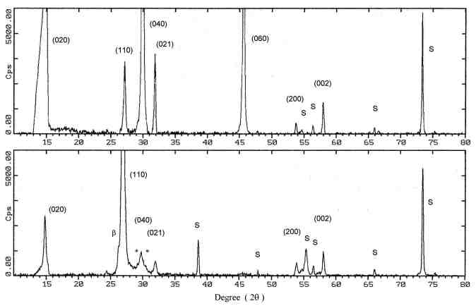
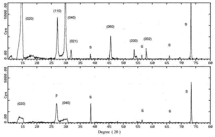
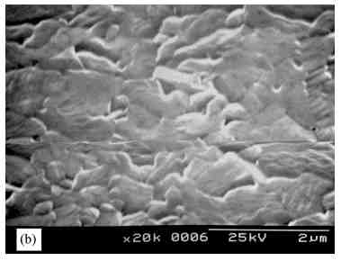
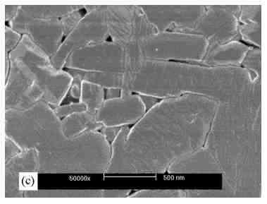
3.1. Microstructure characterization Figure 2 and 3 show the X-ray diffraction spectra of a MoO3 single-layer and a multilayer, respectively. The XRD pattern of the as-deposited MoO3 single-layer (Fig. 2. bottom) indicates a major phase of orthorhombic MoO3 and minor phases of monoclinic b -MoO3 and triclinic Mo9O26. The b -MoO3 is a metastable phase and transforms to the orthorhombic form of MoO3 at elevated temperature above 350°C [8]. The Mo9O26 is an intermediate phase which is known as a form of non-stoichiometric molybdenum trioxide. The XRD pattern indicates also that the film has an (110) orientation, although some reflections corresponding to (010) and (100) planes are observed. After the single-layer film had been annealed in synthetic air, the phase transformations from the b -MoO3 and Mo9O26 to orthorhombic MoO3 occurred, as seen in Fig. 2. top. It is clear when comparing the XRD pattern of the as-deposited film and the annealed film that during the annealing the intensity of the (110) preferred orientation was decreased. The crystallites undergo a reorientation, with increasing the intensity of the (010) peak and then this orientation is the preferred one. The multilayer films (sample B and C) show a similar behavior. The XRD pattern indicate that the as-deposited multilayer film has a major phase of MoO3 and also indicates the formation of b -MoO3 (Fig. 3. bottom). The intensity of the peaks is very low and they show a strong broadening effect. This suggests that the film consists of very small crystallites and the particles are spreading to form a little amorphous contribution to the film on the substrate. The annealing process caused the growth of the crystal, as shown by the increasing intensity of the reflections (Fig. 3. top). The b -MoO3 transformed to orthorhombic MoO3 and the (010) preferential orientation is formed. SEM micrographs of the annealed single
layer and multilayer films are shown in Fig. 4. It is obvious that the
deposition methods have a strong influence on the surface morphology of
the MoO3 films. The structure of the single-layer film can be
characterized as whisker-like (Fig. 4.a). It forms grains which are arranged
in almost independently clusters. The grain length is about the same for
all grains, but the grain thickness is varied and widely distributed. The
structure exposes a very high surface-to-volume ratio.
Fig. 2. the XRD spectra of a MoO3 single-layer on a SiO2/Si substrate: as-deposited film (bottom) and after annealing process (top). The major phase is orthorhombic MoO3. S indicates peaks of the substrate, b and * are the monoclinic MoO3 and Mo9O26, respectively.
Fig. 3. the XRD spectra of a MoO3 multilayer on a SiO2/Si substrate: as-deposited film (bottom) and after annealing process (top). The major phase is orthorhombic MoO3. S indicates peaks of the substrate and b is the monoclinic MoO3.
The multilayer films show a smooth
surface and dense morphology (Fig. 4.b and c). An interpenetrating microstructure
was likely developed, as seen on the film B (deposited using a back - sputtering
power of 250 W). For the film C (deposited using a back - sputtering power
of 750 W), the microstructure consists of fine and several elongated grains
with straight grain boundaries. It also shows a smoothening effect on the
surface by the increased rf-power of the back-sputtering.
Fig. 4. SEM micrographs of the sputtered MoO3 thin films on SiO2/Si substrate after annealing process: (a) single-layer film sample A, (b) multilayer film sample B (deposited with back-sputtering power of 250 W), and (c) multilayer film sample C (deposited with back-sputtering power of 750 W). The dense structure and smoothening effect on the surface of the multilayer films is as a result of a back-sputtering process at each interface during the multilayer deposition. The effect is much more closely associated with the energy of the Ar-ions bombarding the surface of the layers. As seen from XRD pattern, the as-deposited multilayer films have very low peaks intensity and are likely to have amorphous-like structure. However, the bombardment with Ar ions at relatively higher energy during back-sputtering seems to promote interfacial diffusion of atoms. Therefore, the adatoms tend to form a more closely-packed construction through random-walk processes and finally, the periodic structures of the atoms are destroyed. The effect of ion bombardment on short-range disorder has been demonstrated previously [9]. 3.2. Gas-sensing properties
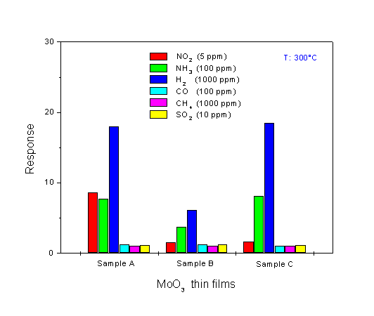
Fig. 5. Response towards various test-gases at 300°C for the MoO3 single-layer (sample A) and multilayer films (sample B and sample C, deposited using a back-sputtering power of 250 W and 750 W, respectively).
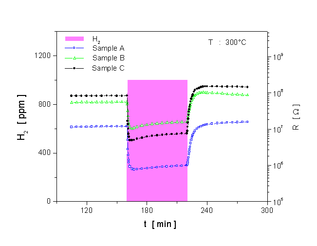
Fig. 6. Dynamic response of the MoO3 films to 1000 ppm H2 at 300°C.
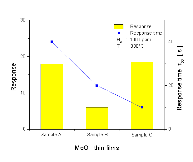
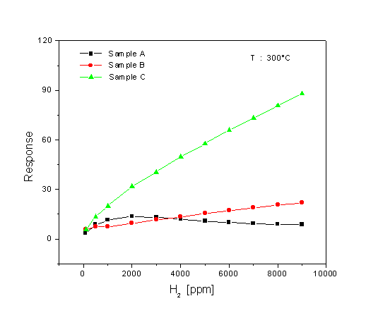
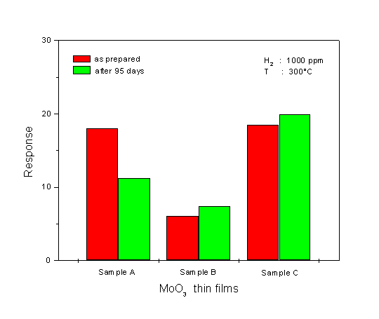
A comparison of the dynamic response to 1000 ppm H2 at 300°C for the three different sensors is shown in Fig. 6. The corresponding data have been used for evaluating the response time of the sensors (see Fig. 7). The response time is defined as the time required for the electrical resistance of the sensors to reach 50% of the equilibrium value following a step increase in H2 gas concentration. As seen in Fig. 6, the single-layer film (sample A) has the best signal shape during exposure to H2. When looking at the result for the response time at Fig. 7, the film shows a slower response time than the multilayer films which have a very fast response time. This very fast response causes an abrupt decrease in resistance, followed by a gradual increase in resistance to reach the equilibrium value. The fastest response time is found for the multilayer film sample C. The H2 response of the sensors at 300°C is plotted as a function of concentration, in Fig. 8. It is obvious that the H2 response is influenced by the microstructure of the films. The MoO3 single-layer shows a saturated response to H2 in a concentration of about 2000 ppm. A good linearity of the response is exposed by the MoO3 multilayer sample B, but the H2 response is low. The MoO3 multilayer sample C shows a very high response to H2 for concentrations ranging from 100 to 9000 ppm. The linearity of the curve is very good in the range of high concentrations between 2000 and 9000 ppm H2. These results prove that the new deposition method for the preparation of MoO3 multilayers can obviously improve the H2 sensing properties compared to conventional MoO3 single-layer thin films. A long-term unenergized storage of a sensor after the first characterization can influence its stability. Figure 9 shows the effect of the unenergized storage period of 95 days on the stability of the H2 response. The single-layer with a very porous structure shows bad stability. After 95 days storage period from its first characterization, the H2 response is reduced from 17 to 10.3. An enhanced stability is found for the multilayer films. A small increase of the H2 response is shown after the storage period. The improvement of the stability may be caused by the dense structure of the multilayer film. Studies of the reduction mechanism
for MoO3 and the surface chemistry of the material during pretreatment
in hydrogen can explain why the MoO3 has a good sensitivity
to H2. Choi et al. [10] have investigated the electronic structure
of MoO3 using XPS before and after hydrogen reduction. After
the reduction by H2 at 400°C, the surface concentration
of M+6 decreased drastically. While 3 h in hydrogen treatment
the Mo+6 concentration was reduced from 100% to 24%. The reduction
of MoO3 involves the reduction from Mo+6 to lower
oxidation states Mo+5 and Mo+4. This result indicates
that the surface of MoO3 is very sensitive to the reduction
by hydrogen.
Fig. 7. Response time of the MoO3 films.
Fig. 8. Comparison of the response of the three MoO3 films to several H2 concentrations at 300°C. Indeed, the gas adsoption is principally
influenced by the microstructure of the film surface. The full width at
half maximum (FWHM) of a peak of the XRD-reflection gives an indication
of the mean crystallite size. The FWHM of the (040) reflection for the
sample A, B, and C after annealing is 0.345, 0.404, and 0.433 deg. The
correlated crystallite sizes of the films are 77, 54, and 47 nm, respectively.
These results indicate that the single-layer film (sample A) has the largest
crystallite size and the multilayer film deposited using a back-sputtering
power of 750 W (sample C) has the smallest crystallites. A remarkable observation
is that the crystallite size is much smaller than the principal physical
structure size as seen on the SEM micrographs (Fig. 4). This indicates
that each of the grains (column tops) seen by SEM may consist of subgrains
[11].
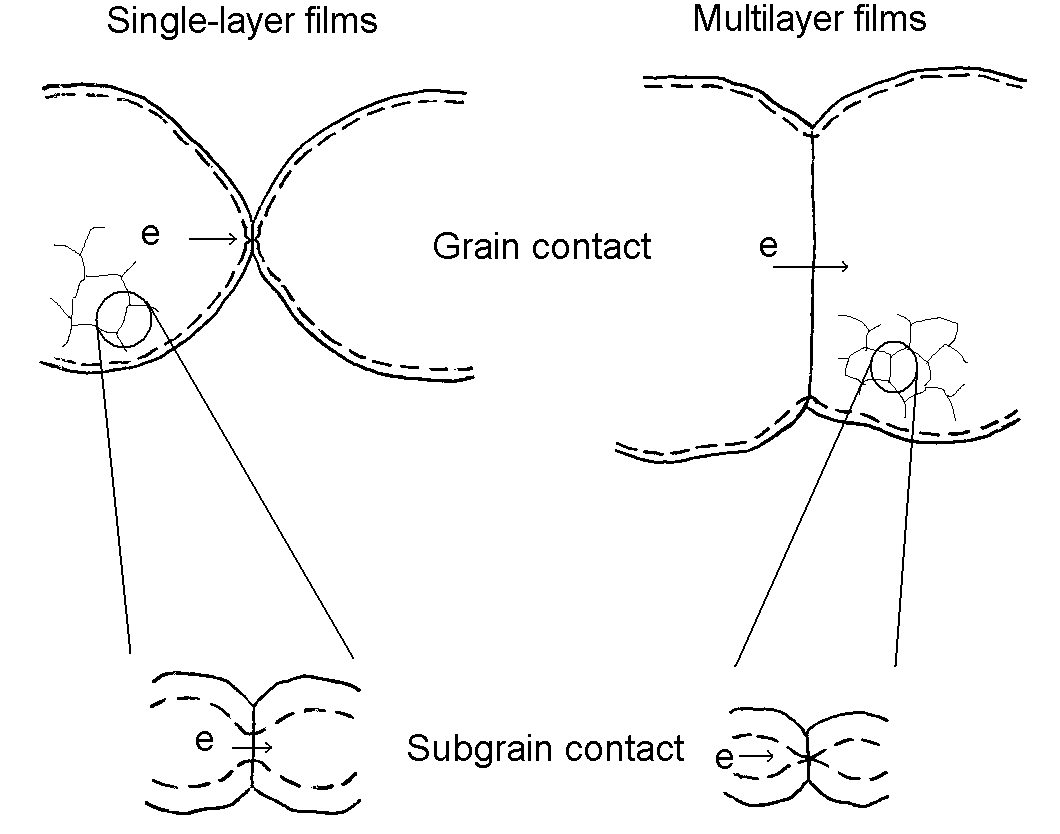
Fig. 9. Effect of the unenergized storage for 95 days on the sensitivity of the MoO3 films. Considering the mechanism of conduction by a porous body like a thin film needs to take account of the structural inhomogeneity, which implies a lower resistance path through the bulk of crystallites alternating with higher resistance constrictions at the point contacts. That means, the grain boundary contacts are most resistive for conducting electrons so that they govern electric resistance of the films as well as the gas sensitivity [12]. The effects of crystallite size on the sensitivity were also shown by Suzuki et al. [13]. Ogawa et al. [14] have proposed that the mobility modulation effect is strongly related to the crystallite size of the thin films and has an effect on the sensitivity of the film towards reduced gas. Based on the microstructure of the
MoO3 thin films which each of their grains consist of subgrains,
we propose two models for conductance limited by intergrain constrictions
as shown in Fig.10. In each of both the depletion layer represents a substantial
fraction of the material comprising the intergrain contact. For the single-layer
film (sample A), the depletion zones from the two surfaces are quasi-overlap,
leaving a high resistance ohmic path across the grain boundary. Within
the two subgrains the depletion zone shows a wide channel across the boundary
and causes a large conductivity. So, the electric resistance of the single-layer
film is dominated by the intergrain contact. On the other hand, for the
multilayer film the subgrain boundary contacts are very resistant to electron
conduction through the chain, so that they govern the electric resistance
as well as the gas sensitivity of the film.
Fig. 10. Schematic model for limited conductance by intergrain restrictions for the single-layer and multilayer MoO3 films.
4. Conclusions
Gas-sensing characteristics of the
films prove that this new preparation method can improve the H2
sensing properties such as sensitivity, selectivity, response time and
long-term stability of the conventionally sputtered MoO3 single-layer
film. The cross-sensitivity towards NO2, NH3, CO,
CH4, and SO2 is low. The response time (t50)
to H2 can be drastically reduced from 40 s for the single-layer
film to 10 s for the multilayer films. The sensor exposes a very high response
to H2 with a good signal linearity in the range of high concentrations
between 2000 and 9000 ppm.
Acknowledgements
References
Biographies
Harald Steffes received his Dipl.-Phys. degree (M.Sc. in physics) from the University of Kaiserslautern in1997. Since May of 1998 he has been a member of the Microsensor & Actuator Technology Center of the Technical University of Berlin. He is currently working towards his Ph.D. in the field of solid state gas sensors. Florian Solzbacher studied in U.K., Germany and Utah, USA. He received his M.Sc. degree in Electrical Engineering from the Technical University Berlin in 1997. Since August 1997 he has been studying as a Ph.D. student at the Microsensor and Actuator Technology Center at the Technical University Berlin. His field of interest covers chemical sensors, biomedical engineering and III-V semiconductors. Ernst Obermeier
received his M.Sc. and Ph.D. degrees in electrical engineering from the
Technical University of Munich in 1977 and 1983, respectively. He worked
as a research scientist at the Fraunhofer Institute in Munich from 1977
to 1988. Since 1988 Professor Obermeier has been the head of the Microsensor
and Actuator Technology Center at the Technical University Berlin. His
research is focused on silicon technology, simulation and modeling of micromachined
sensors and the development of chemical and high-temperature sensors.
This paper is accepted for publishing in Journal of Sensors and Actuators, January 2001
Artikel ini dimuat di Majalah Elektronik Ilmiah FDIB edisi Januari 20001 dengan ijin penulis pertama. https://fdib.tripod.com/e-zine/ez-cuk.html . |
|||||||||||||||||||||||||||||||||||||||||||||||||||||||||||||||
| KEMBALI- | --- | -- | |||||||||||||||||||||||||||||||||||||||||||||||||||||||||||||